logo
Products
PRODUCTS DETAILS
Home > Products >
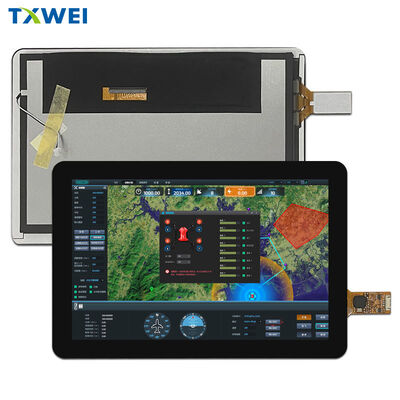
Capacitive Touch 8-Inch LVDS Display Module 1920x1200 G+G USB Panel 1000nits

Capacitive Touch 8-Inch LVDS Display Module 1920x1200 G+G USB Panel 1000nits

MOQ: 1 Piece
Price: USD 25-45 / Piece
Standard Packaging: Anti-static bag with shock-proof foam insert, export-grade corrugated carton
Delivery Period: 3-7 working days for samples, 15-25 days for mass production
Payment Method: T/T,L/C,PayPal,Western Union
Supply Capacity: 50000 Pieces per Month
Detail Information
Place of Origin
Guangdong, China
Brand Name
TXW
Certification
RoHS, ISO 9001:2015
Model Number
TXW800035B1-TY
Display Size:
8.0 Inch
Resolution:
1920 X RGB X 1200 Dots (WUXGA)
Aspect Ratio:
16:10 Landscape
Pixel Density:
~283 PPI
LCD Type:
TFT Active Matrix, Normally Black
Video Interface:
LVDS (odd/even Channels)
Viewing Direction:
ALL (80/80/80/80)
Pixel Pitch:
0.0897 X 0.0897 Mm
Active Area:
172.22 X 107.64 Mm
Module Size:
197.50 X 132.30 X 6.85 Mm
Brightness:
1000 Cd/m2 Typ / 1200 Cd/m2 Max
Uniformity:
70% (Min)
Backlight:
36 White LEDs, 330mA Typ, 16.8-19.2V
LED Life Time:
20000 Hours
Touch Structure:
G+G Capacitive, ILI2132, USB HID
Touch Transmittance:
>=85%
Touch Hardness:
>=6H
Supply Voltage:
3.3V (Typ.)
Operating Temperature:
-30C To +85C
Storage Temperature:
-30C To +85C
Certification:
RoHS
Highlight:

8-inch capacitive touch display module

,

LVDS display panel 1920x1200

,

G+G USB LCD module 1000nits

Product Description
Technical Design Brief  ·  TXW800035B1-TY

The Wide-Format HMI Display, Reconsidered: Engineering 1920×1200 LVDS Touch into an 8-Inch Platform

A differentiated engineering brief on signal integrity, capacitive sensing architecture, optical lamination, and thermal derating — written for design teams who specify the panel, not merely purchase it.

8.0″ WUXGA 1920×1200 16:10 LVDS G+G USB Touch 1000 cd/m² -30°C ~ +85°C
16:10
Wide Format
283 PPI
Pixel Density
1920×1200
WUXGA
1000
cd/m² Typ
-30~+85°C
Operating Range
USB
Plug-and-Play Touch

1   The Wide-Format Problem Space

Human factors and pixel geometry are inseparable. At an 8.0-inch diagonal, a 1920×1200 matrix resolves to approximately 283 pixels per inch (√(1920²+1200²)/8.0). That density sits well above the threshold at which a normally-sighted operator resolves discrete pixel structure at typical HMI viewing distances of 30–70 cm, so vector UI elements and small glyphs render without perceptible aliasing.

The 16:10 ratio (1.60) is not arbitrary. It approaches the golden ratio (φ ≈ 1.618), and its area-to-perimeter economics favor the dense, multi-column layouts — a trend chart beside a setpoint table beside a control cluster — that define industrial and medical software. Where a 4:3 panel forces vertical stacking and scrolling, the wide canvas lets information coexist spatially, reducing operator navigation cost.

Design implication: specify 16:10 when the dominant UI gesture is horizontal comparison; reserve portrait terrains for form entry and long lists.

2   Signal Integrity: Why LVDS Serialization Wins

LVDS (TIA/EIA-644) converts a wide single-ended pixel bus into a small constellation of low-swing differential pairs. The canonical 7:1 mapping folds seven single-ended bits onto one differential line, so a 24-bit RGB bus with timing collapses from roughly 28 conductors into five pairs — here organized as odd/even channel groups (ELV0-3 / OLV0-3 plus clocks).

The engineering consequences compound. A controlled common-mode near 1.2 V with a ≈350 mV differential swing yields fast transition edges at comparatively low dynamic power (P ∝ C·V²·f). Tightly coupled pairs cancel far-field fields, suppressing common-mode radiation; and the modest swing keeps the eye diagram open across the connector and flex without receiver equalization. For an 8-inch panel crossing dozens of centimeters of internal harness, that margin is the difference between a robust design and an intermittent one.

EMC discipline: preserve differential-pair length matching, maintain uninterrupted reference-ground return, and terminate with the specified characteristic impedance. The module provides steel-plate grounding reinforcement to anchor these returns mechanically.

3   Toward a G+G Capacitive Sensing Architecture

The module adopts a glass-on-glass (G+G) construction: a discrete ITO sensor glass laminated beneath a separate cover glass. This separates the sensing substrate from the structural front glass, allowing each to be optimized — the sensor for electrode geometry and optical neutrality, the cover for hardness and impact resistance.

Sensing is mutual-capacitive. Transmit electrodes are energized while receive electrodes measure the charge coupled at every intersection; a fingertip diverts a portion of the fringing field, producing a localized ΔC that the controller resolves into a centroid. The ILI2132 front-end reports standardized USB HID digitizer packets, so the host enumerates a native touch device without bespoke driver development — an integration shortcut with real engineering value.

Noise & ESD posture: keep the sensor's ground return low-impedance, route switching supplies away from the sensor tail, and provide perimeter ESD clamps. Capacitive front-ends trade elegantly with contamination and wear, but are sensitive to poor return paths.

4   The Optical Stack: Lamination, AF/AG, and the Clarity–Haze Trade-off

Every unbonded air interface creates a Fresnel reflection of roughly 4% per surface, plus an internal light-guide path that scatters ambient light. Optically bonding the stack — cover glass to sensor via SCA, sensor to panel via OCA — removes those interfaces, raising effective contrast under bright light, attenuating internal reflection artifacts, and adding mechanical stiffness against shock and contamination ingress.

The cover lens then carries two engineered surface functions: an anti-fingerprint (AF) layer that lowers surface energy to resist oleophobic smudging, and anti-glare (AG) etching that scatters specular highlights into a matte field. The design achieves ≥85% transmittance and ≥6H hardness while retaining optical clarity.

The clarity–haze dialectic: AG reduces specular glare at the cost of slight image diffusion. In bright, directionally-lit environments the net legibility gain dominates; in dark control rooms, minimal-haze finishes are preferred.

5   Photometry and the Physics of Lifetime Derating

The edge-lit backlight aggregates 36 white LEDs feeding a light-guide plate, delivering 1000 cd/m² typical (1200 cd/m² maximum) with 70% minimum uniformity. Luminance headroom is the operative metric for high-ambient systems: it preserves the display's effective contrast ratio when additive ambient reflection compresses the dark end of the transfer curve.

Rated LED life is 20,000 hours, defined as the interval to 50% of initial luminance at 55 mA/LED. Luminous depreciation accelerates with junction temperature, and the drive current couples directly into that temperature. Sustaining the rated life therefore demands thermal design — adequate rear heat-spreading and attention to enclosure ventilation — not merely electrical compliance.

6   Electrical Architecture and Power Sequencing

The module runs from a 3.3 V VDDIN rail that feeds an on-module DC/DC stage generating the panel's internal gate/source supplies; the backlight is a separate high-compliance string (VF 16.8–19.2 V at IF 330 mA typical / 390 mA max, 36 LEDs). A constant-current LED driver is essential to immunize luminance against VF binning and thermal drift; PWM or analog dimming extends the usable brightness range without chromatic shift.

Sequencing guidance: assert VDDIN before driving the backlight; de-assert the backlight first on power-down. Respect logic and analog rails' ramp order to avoid latch-up and residual in-panel charge.

7   Reliability Qualification Matrix

Test ItemCondition
High-Temperature Storage+85°C / 96 H
Low-Temperature Storage-30°C / 96 H
High-Temperature Operating+85°C / 96 H
Low-Temperature Operating-30°C / 96 H
High-Temperature / Humidity Storage60°C × 90%RH / 96 H
Thermal and Cold Shock-30°C (30 min) ↔ +85°C (30 min), 10 cycles

Pass criteria exclude functional anomalies, missing or shorted segments, clarity degradation, non-display states, and liquid-crystal leakage — the module must retain electrical and optical integrity across the entire envelope.

8   Integration Engineering Notes

Touch-window sizing. Increase the cover-lens window unilaterally by 0.3–0.5 mm relative to the LCD active area to absorb bonding tolerance.
Mechanical routing. Observe the specified FPC bend profile; the connector is a 1.0 mm pitch front-insertion flipper, and the module ships with the touch flex dressed on the backlight.
Thermal & EMC. Anchor the steel grounding plate to chassis; keep the LED string's thermal path short; maintain pair-to-pair isolation for LVDS.

9   Comparative Analysis

DimensionThis ModuleConventional Alternative
Resolution & format1920×1200 WUXGA, 16:10, ~283 PPILower-res 4:3 / 16:9; coarser PPI
Video linkLVDS differential serial, low EMI, few conductorsParallel RGB: wide, EMI-prone bus
TouchG+G capacitive, ILI2132, USB HIDResistive, or I2C touch needing firmware
Optical stackFull lamination, AF+AG, ≥85% T, ≥6HAir-gap, untreated lens
Thermal envelope-30°C to +85°CNarrower consumer range

10   Application Domains

Self-service kiosks and ticketing terminals · retail POS and interactive merchandising · industrial control panels and machine HMIs · medical monitors and diagnostic front panels · in-vehicle, EV, and charging-station terminals · digital signage and smart-building control hubs.

11   Frequently Asked Questions

Why 16:10 rather than 16:9?
16:10 grants additional vertical pixel budget that eases multi-row dashboards and text rendering, while remaining wide enough for horizontal comparison layouts.
Why USB touch instead of I2C?
USB HID enumeration removes touch-driver development and firmware integration, shortening time-to-first-image on most host platforms.
Is the module sunlight-readable?
1000 cd/m² typical brightness, full lamination, and AG surface treatment together preserve effective contrast in high-ambient settings.
What drives the rated LED lifetime?
Luminous depreciation to 50% at 55 mA/LED; higher current and junction temperature shorten it, making thermal design decisive.

Engage the Design-in Team

Evaluate the TXW800035B1-TY with samples, full datasheets, and OEM/ODM customization across FPC, cover lens, interfaces, and backlight topology.

Contact us for samples and pricing — and bring your enclosure constraints early; co-optimizing stack-up, grounding, and thermals is where we add the most value.

Products
PRODUCTS DETAILS
Capacitive Touch 8-Inch LVDS Display Module 1920x1200 G+G USB Panel 1000nits
MOQ: 1 Piece
Price: USD 25-45 / Piece
Standard Packaging: Anti-static bag with shock-proof foam insert, export-grade corrugated carton
Delivery Period: 3-7 working days for samples, 15-25 days for mass production
Payment Method: T/T,L/C,PayPal,Western Union
Supply Capacity: 50000 Pieces per Month
Detail Information
Place of Origin
Guangdong, China
Brand Name
TXW
Certification
RoHS, ISO 9001:2015
Model Number
TXW800035B1-TY
Display Size:
8.0 Inch
Resolution:
1920 X RGB X 1200 Dots (WUXGA)
Aspect Ratio:
16:10 Landscape
Pixel Density:
~283 PPI
LCD Type:
TFT Active Matrix, Normally Black
Video Interface:
LVDS (odd/even Channels)
Viewing Direction:
ALL (80/80/80/80)
Pixel Pitch:
0.0897 X 0.0897 Mm
Active Area:
172.22 X 107.64 Mm
Module Size:
197.50 X 132.30 X 6.85 Mm
Brightness:
1000 Cd/m2 Typ / 1200 Cd/m2 Max
Uniformity:
70% (Min)
Backlight:
36 White LEDs, 330mA Typ, 16.8-19.2V
LED Life Time:
20000 Hours
Touch Structure:
G+G Capacitive, ILI2132, USB HID
Touch Transmittance:
>=85%
Touch Hardness:
>=6H
Supply Voltage:
3.3V (Typ.)
Operating Temperature:
-30C To +85C
Storage Temperature:
-30C To +85C
Certification:
RoHS
Minimum Order Quantity:
1 Piece
Price:
USD 25-45 / Piece
Packaging Details:
Anti-static bag with shock-proof foam insert, export-grade corrugated carton
Delivery Time:
3-7 working days for samples, 15-25 days for mass production
Payment Terms:
T/T,L/C,PayPal,Western Union
Supply Ability:
50000 Pieces per Month
Highlight

8-inch capacitive touch display module

,

LVDS display panel 1920x1200

,

G+G USB LCD module 1000nits

Product Description
Technical Design Brief  ·  TXW800035B1-TY

The Wide-Format HMI Display, Reconsidered: Engineering 1920×1200 LVDS Touch into an 8-Inch Platform

A differentiated engineering brief on signal integrity, capacitive sensing architecture, optical lamination, and thermal derating — written for design teams who specify the panel, not merely purchase it.

8.0″ WUXGA 1920×1200 16:10 LVDS G+G USB Touch 1000 cd/m² -30°C ~ +85°C
16:10
Wide Format
283 PPI
Pixel Density
1920×1200
WUXGA
1000
cd/m² Typ
-30~+85°C
Operating Range
USB
Plug-and-Play Touch

1   The Wide-Format Problem Space

Human factors and pixel geometry are inseparable. At an 8.0-inch diagonal, a 1920×1200 matrix resolves to approximately 283 pixels per inch (√(1920²+1200²)/8.0). That density sits well above the threshold at which a normally-sighted operator resolves discrete pixel structure at typical HMI viewing distances of 30–70 cm, so vector UI elements and small glyphs render without perceptible aliasing.

The 16:10 ratio (1.60) is not arbitrary. It approaches the golden ratio (φ ≈ 1.618), and its area-to-perimeter economics favor the dense, multi-column layouts — a trend chart beside a setpoint table beside a control cluster — that define industrial and medical software. Where a 4:3 panel forces vertical stacking and scrolling, the wide canvas lets information coexist spatially, reducing operator navigation cost.

Design implication: specify 16:10 when the dominant UI gesture is horizontal comparison; reserve portrait terrains for form entry and long lists.

2   Signal Integrity: Why LVDS Serialization Wins

LVDS (TIA/EIA-644) converts a wide single-ended pixel bus into a small constellation of low-swing differential pairs. The canonical 7:1 mapping folds seven single-ended bits onto one differential line, so a 24-bit RGB bus with timing collapses from roughly 28 conductors into five pairs — here organized as odd/even channel groups (ELV0-3 / OLV0-3 plus clocks).

The engineering consequences compound. A controlled common-mode near 1.2 V with a ≈350 mV differential swing yields fast transition edges at comparatively low dynamic power (P ∝ C·V²·f). Tightly coupled pairs cancel far-field fields, suppressing common-mode radiation; and the modest swing keeps the eye diagram open across the connector and flex without receiver equalization. For an 8-inch panel crossing dozens of centimeters of internal harness, that margin is the difference between a robust design and an intermittent one.

EMC discipline: preserve differential-pair length matching, maintain uninterrupted reference-ground return, and terminate with the specified characteristic impedance. The module provides steel-plate grounding reinforcement to anchor these returns mechanically.

3   Toward a G+G Capacitive Sensing Architecture

The module adopts a glass-on-glass (G+G) construction: a discrete ITO sensor glass laminated beneath a separate cover glass. This separates the sensing substrate from the structural front glass, allowing each to be optimized — the sensor for electrode geometry and optical neutrality, the cover for hardness and impact resistance.

Sensing is mutual-capacitive. Transmit electrodes are energized while receive electrodes measure the charge coupled at every intersection; a fingertip diverts a portion of the fringing field, producing a localized ΔC that the controller resolves into a centroid. The ILI2132 front-end reports standardized USB HID digitizer packets, so the host enumerates a native touch device without bespoke driver development — an integration shortcut with real engineering value.

Noise & ESD posture: keep the sensor's ground return low-impedance, route switching supplies away from the sensor tail, and provide perimeter ESD clamps. Capacitive front-ends trade elegantly with contamination and wear, but are sensitive to poor return paths.

4   The Optical Stack: Lamination, AF/AG, and the Clarity–Haze Trade-off

Every unbonded air interface creates a Fresnel reflection of roughly 4% per surface, plus an internal light-guide path that scatters ambient light. Optically bonding the stack — cover glass to sensor via SCA, sensor to panel via OCA — removes those interfaces, raising effective contrast under bright light, attenuating internal reflection artifacts, and adding mechanical stiffness against shock and contamination ingress.

The cover lens then carries two engineered surface functions: an anti-fingerprint (AF) layer that lowers surface energy to resist oleophobic smudging, and anti-glare (AG) etching that scatters specular highlights into a matte field. The design achieves ≥85% transmittance and ≥6H hardness while retaining optical clarity.

The clarity–haze dialectic: AG reduces specular glare at the cost of slight image diffusion. In bright, directionally-lit environments the net legibility gain dominates; in dark control rooms, minimal-haze finishes are preferred.

5   Photometry and the Physics of Lifetime Derating

The edge-lit backlight aggregates 36 white LEDs feeding a light-guide plate, delivering 1000 cd/m² typical (1200 cd/m² maximum) with 70% minimum uniformity. Luminance headroom is the operative metric for high-ambient systems: it preserves the display's effective contrast ratio when additive ambient reflection compresses the dark end of the transfer curve.

Rated LED life is 20,000 hours, defined as the interval to 50% of initial luminance at 55 mA/LED. Luminous depreciation accelerates with junction temperature, and the drive current couples directly into that temperature. Sustaining the rated life therefore demands thermal design — adequate rear heat-spreading and attention to enclosure ventilation — not merely electrical compliance.

6   Electrical Architecture and Power Sequencing

The module runs from a 3.3 V VDDIN rail that feeds an on-module DC/DC stage generating the panel's internal gate/source supplies; the backlight is a separate high-compliance string (VF 16.8–19.2 V at IF 330 mA typical / 390 mA max, 36 LEDs). A constant-current LED driver is essential to immunize luminance against VF binning and thermal drift; PWM or analog dimming extends the usable brightness range without chromatic shift.

Sequencing guidance: assert VDDIN before driving the backlight; de-assert the backlight first on power-down. Respect logic and analog rails' ramp order to avoid latch-up and residual in-panel charge.

7   Reliability Qualification Matrix

Test ItemCondition
High-Temperature Storage+85°C / 96 H
Low-Temperature Storage-30°C / 96 H
High-Temperature Operating+85°C / 96 H
Low-Temperature Operating-30°C / 96 H
High-Temperature / Humidity Storage60°C × 90%RH / 96 H
Thermal and Cold Shock-30°C (30 min) ↔ +85°C (30 min), 10 cycles

Pass criteria exclude functional anomalies, missing or shorted segments, clarity degradation, non-display states, and liquid-crystal leakage — the module must retain electrical and optical integrity across the entire envelope.

8   Integration Engineering Notes

Touch-window sizing. Increase the cover-lens window unilaterally by 0.3–0.5 mm relative to the LCD active area to absorb bonding tolerance.
Mechanical routing. Observe the specified FPC bend profile; the connector is a 1.0 mm pitch front-insertion flipper, and the module ships with the touch flex dressed on the backlight.
Thermal & EMC. Anchor the steel grounding plate to chassis; keep the LED string's thermal path short; maintain pair-to-pair isolation for LVDS.

9   Comparative Analysis

DimensionThis ModuleConventional Alternative
Resolution & format1920×1200 WUXGA, 16:10, ~283 PPILower-res 4:3 / 16:9; coarser PPI
Video linkLVDS differential serial, low EMI, few conductorsParallel RGB: wide, EMI-prone bus
TouchG+G capacitive, ILI2132, USB HIDResistive, or I2C touch needing firmware
Optical stackFull lamination, AF+AG, ≥85% T, ≥6HAir-gap, untreated lens
Thermal envelope-30°C to +85°CNarrower consumer range

10   Application Domains

Self-service kiosks and ticketing terminals · retail POS and interactive merchandising · industrial control panels and machine HMIs · medical monitors and diagnostic front panels · in-vehicle, EV, and charging-station terminals · digital signage and smart-building control hubs.

11   Frequently Asked Questions

Why 16:10 rather than 16:9?
16:10 grants additional vertical pixel budget that eases multi-row dashboards and text rendering, while remaining wide enough for horizontal comparison layouts.
Why USB touch instead of I2C?
USB HID enumeration removes touch-driver development and firmware integration, shortening time-to-first-image on most host platforms.
Is the module sunlight-readable?
1000 cd/m² typical brightness, full lamination, and AG surface treatment together preserve effective contrast in high-ambient settings.
What drives the rated LED lifetime?
Luminous depreciation to 50% at 55 mA/LED; higher current and junction temperature shorten it, making thermal design decisive.

Engage the Design-in Team

Evaluate the TXW800035B1-TY with samples, full datasheets, and OEM/ODM customization across FPC, cover lens, interfaces, and backlight topology.

Contact us for samples and pricing — and bring your enclosure constraints early; co-optimizing stack-up, grounding, and thermals is where we add the most value.

sitemap |  Privacy Policy | China Good Quality TFT LCD Display Supplier. Copyright © 2024-2026 Shenzhen Tianxianwei Technology Co., Ltd. . All Rights Reserved.